|
|
|
Kategorie
|
|
Informacje
|
|
Polecamy
|
|
|
 |
|
|
Dla tego produktu nie napisano jeszcze recenzji!
 ;
Szybko, sprawnie i tanio. Serwis godny polecenia. Będę polecał innym
 ;
Ogólnie jest OK, z wyjątkiem obrazu płyty głównej, który jest miejscami mało czytelny, ale można sobie poradzić.
;
Dokładna dokumentacja, pomogła w szybkiej naprawie telewizora. Dziękuję!
;
jedyne do czego mogę mieć zastrzeżenie to jakość zdjęć zawartych w przesłanej instrukcji serwisowej ponieważ są fatalnej jakości, praktycznie nieczytelne. tak poza tym jestem zadowolony to jest to czego szukałem.
;
Wszystko w porządku.
Instrukcja czytelna i kompletna.
Dziękuję.
all right!
thank you.
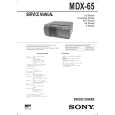
MDX-65
THIS NOTE IS COMMON FOR PRINDED WIRING BOARDS AND SCHEMATIC DIAGRAMS. (In addition to this, the necessary note is printed in each block.) for schematic diagrams � All capacitors are in µF unless otherwise noted. pF: µµF 50 WV or less are not indicated except for electrolytics and tantalums. � All resistors are in � and 1/4 W or less unless otherwise specified. � % : indicates tolerance. � C : panel designation. Note: The components identified by mark ! or dotted line with mark ! are critical for safety. Replace only with part number specified. Note: Les composants identifiés par une marque ! sont critiques pour la sécurité. Ne les remplacer que par une piéce portant le numéro spécifié.
4-4. PRINTED WIRING BOARDS � SERVO SECTION �
� U : B+ Line. � Power voltage is dc 14.4V and fed with regulated dc power supply from Master unit. � Voltage and waveforms are dc with respect to ground under no-signal conditions. no mark : PB � : Impossible to measure � Voltages are taken with a VOM (Input impedance 10 M�). Voltage variations may be noted due to normal production tolerances. � Waveforms are taken with a oscilloscope. Voltage variations may be noted due to normal production tolerances. � Circled numbers refer to waveforms. � Signal path. E : PB for printed wiring boards � X : parts extracted from the component side. � Y : parts extracted from the conductor side. � r : Through hole. � b : Pattern from the side which enables seeing. (The other layer�s patterns are not indicated.) Caution: Pattern face side: (Side B) Parts face side: (Side A) Parts on the pattern face side seen from the pattern face are indicated. Parts on the parts face side seen from the parts face are indicated.
� 17 �
� 18 �
|
|
|
> |
|