|
|
|
Kategorie
|
|
Informacje
|
|
Polecamy
|
|
|
 |
|
|
Dla tego produktu nie napisano jeszcze recenzji!
 ;
jedyne do czego mogę mieć zastrzeżenie to jakość zdjęć zawartych w przesłanej instrukcji serwisowej ponieważ są fatalnej jakości, praktycznie nieczytelne. tak poza tym jestem zadowolony to jest to czego szukałem.
 ;
Wszystko w porządku.
Instrukcja czytelna i kompletna.
Dziękuję.
all right!
thank you.
;
Bardzo dobra instrukcja. Zawiera wszystko co potrzeba, polecam!
;
Instrukcja jest OK. Schematy czytelne, opisane niektóre procedury.
;
Instrukcja bardzo czytelna. zawiera co potrzeba. Polecam
SA-WM500
Ver 1.1 2003.06
SECTION 2 DIAGRAMS
THIS NOTE IS COMMON FOR PRINTED WIRING BOARDS AND SCHEMATIC DIAGRAMS. (In addition to this, the necessary note is printed in each block.)
For Printed Wiring Boards. Note : � X : parts extracted from the component side. � x : parts extracted from the conductor side. � : Pattern from the side which enables seeing. For Schematic Diagrams. Note: � All capacitors are in µF unless otherwise noted. pF: µµF 50 WV or less are not indicated except for electrolytics and tantalums. � All resistors are in � and 1/4 W or less unless otherwise specified. � C : panel designation. Note: The components identified by mark 0 or dotted line with mark 0 are critical for safety. Replace only with part number specified. � � � � � Note: Les composants identifiés par une marque 0 sont critiques pour la sécurité. Ne les remplacer que par une piéce portant le numéro spécifié.
A : B+ Line. B : B� Line. Voltages are dc with respect to ground under no-signal conditions. no mark : Power on Voltages are taken with a VOM (Input impedance 10 M�). Voltage variations may be noted due to normal production tolerances. � Signal path. F : AUDIO � Abbreviation CND : Canadian model MY : Malaysia model SP : Singapore model AUS : Australian model TW : Taiwan model
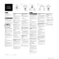
2-1. CIRCUIT BOARDS LOCATION
CONTROL board
MAIN board
POWER AMP board
POWER SUPPLY board
LED board
POWER SWITCH board
4
|
|
|
> |
|